Semiconductor
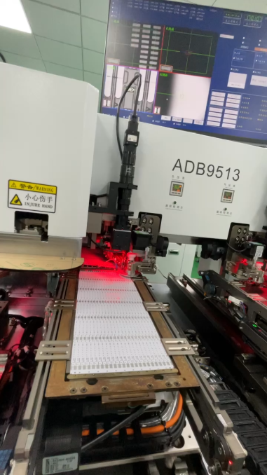
Widely used in the semiconductor industry for material bonding between chip packages and encapsulations.
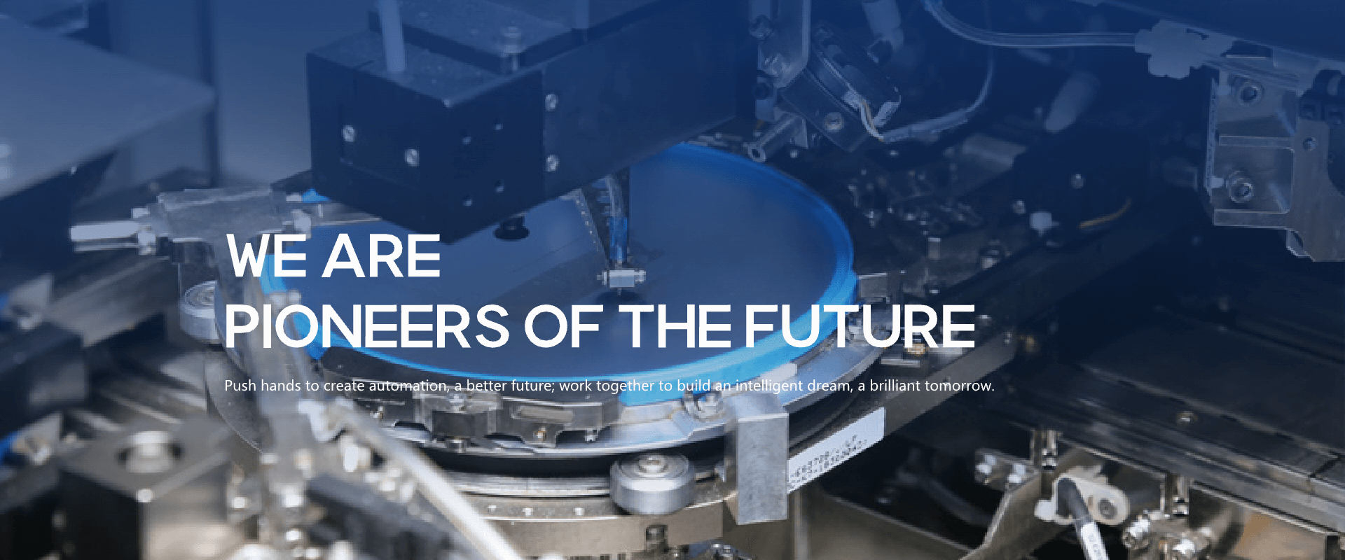
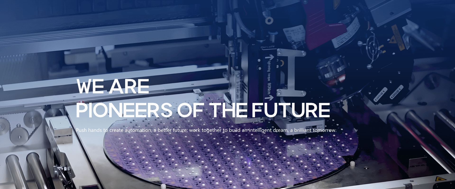
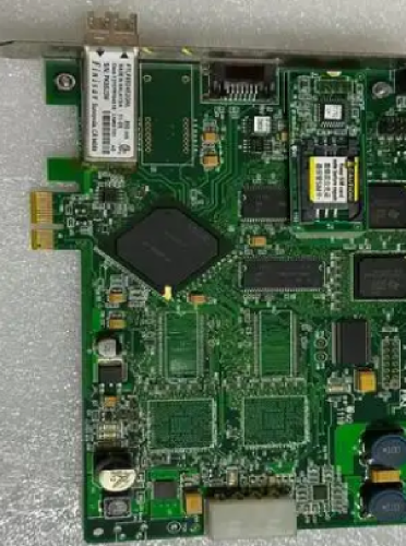
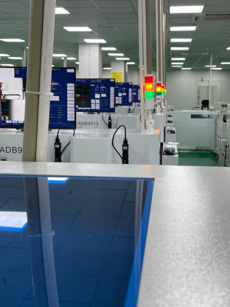
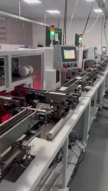
Shenzhen Huagao Automation Equipment Co., Ltd. is located in Bao'an District, Shenzhen, the capital of innovation. It focuses on chip, LED and semiconductor packaging equipment, and is a high-end intelligent equipment manufacturer integrating research, production and sales.
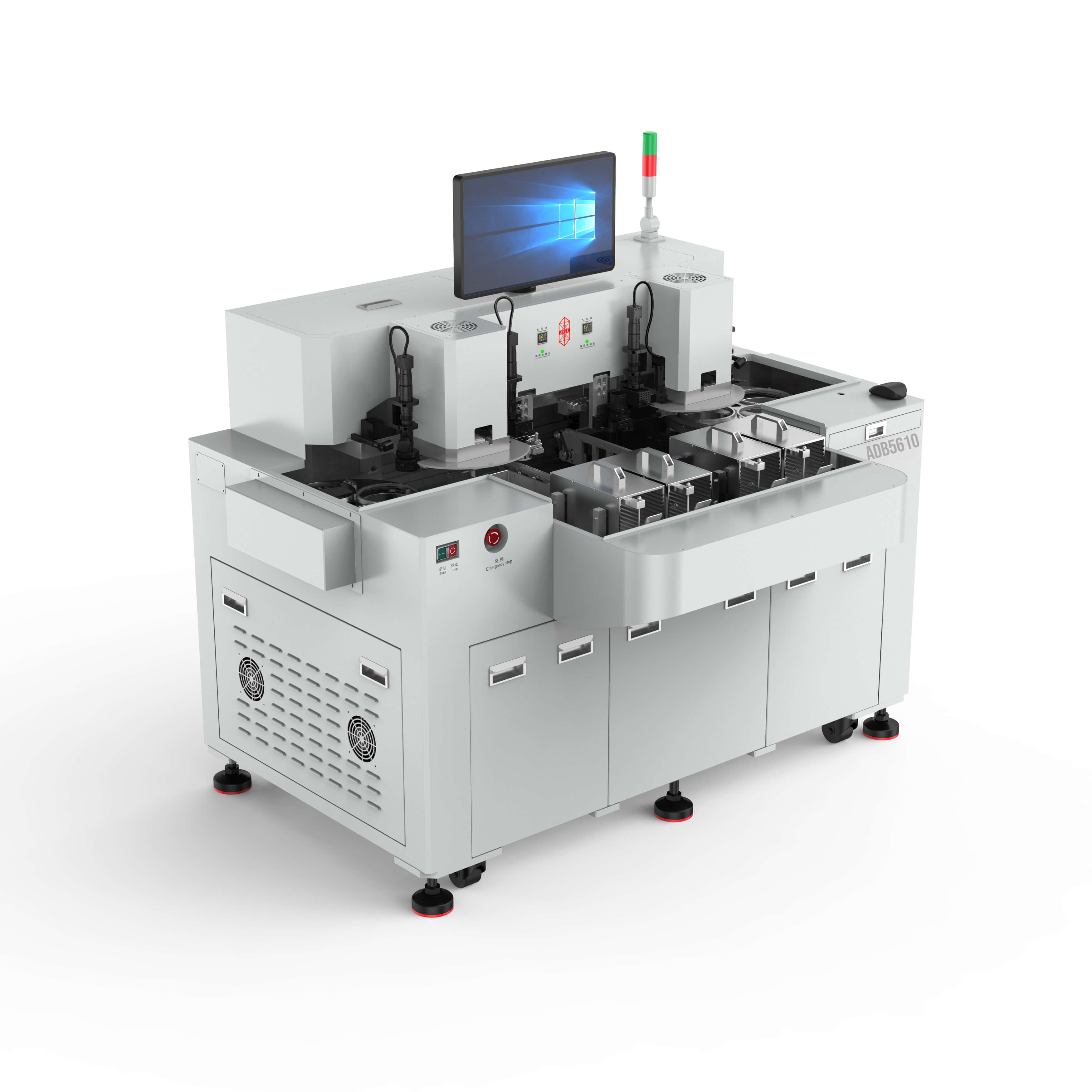
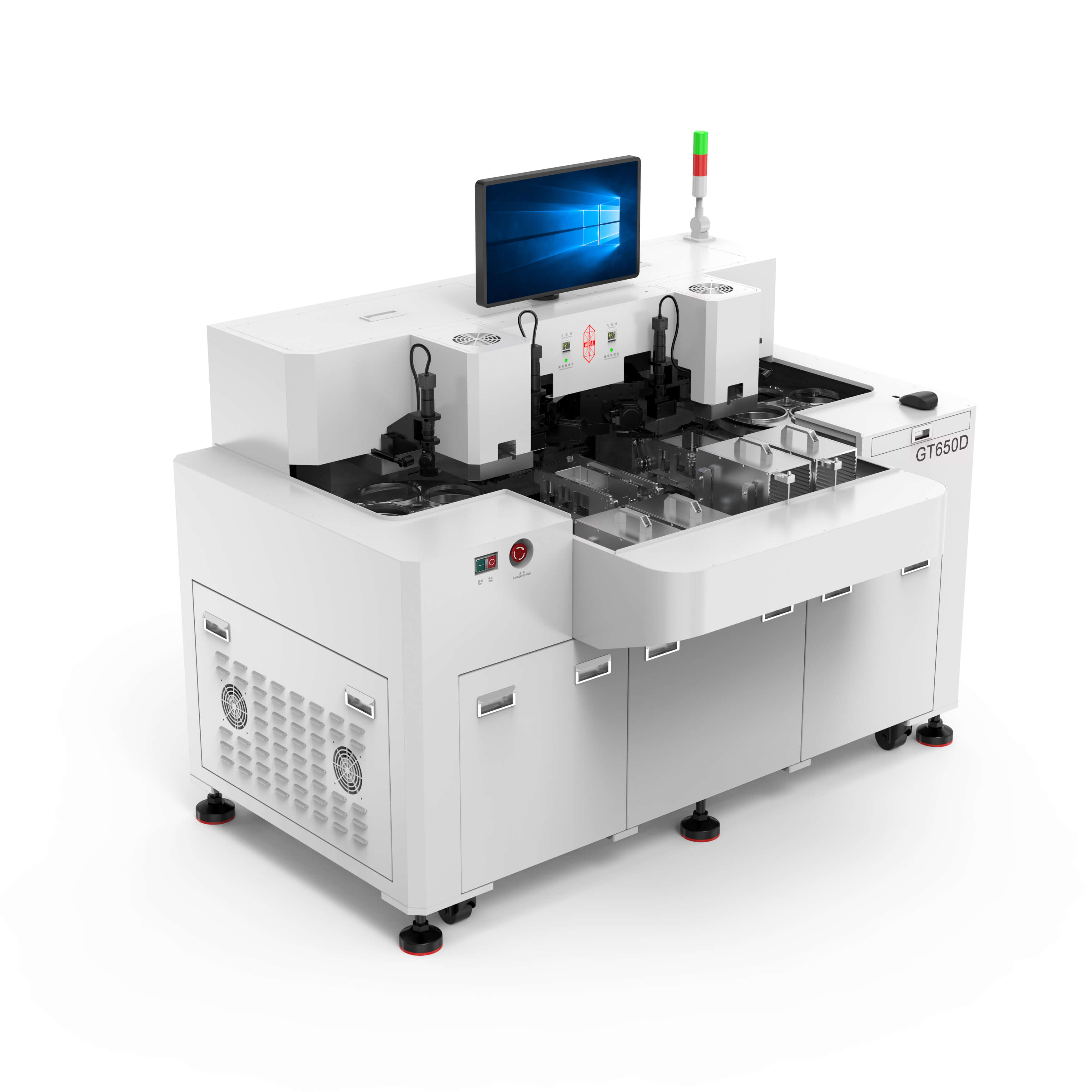
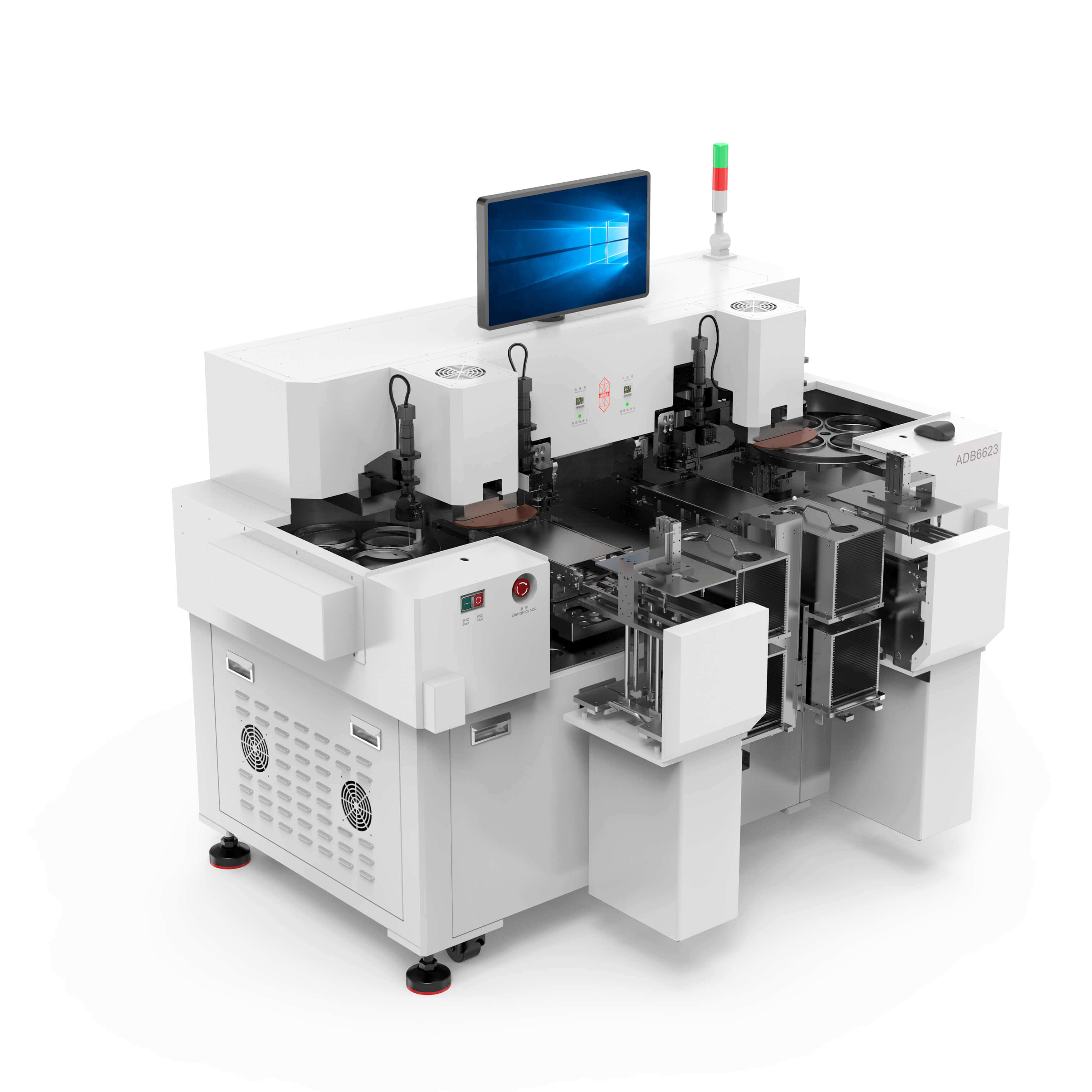
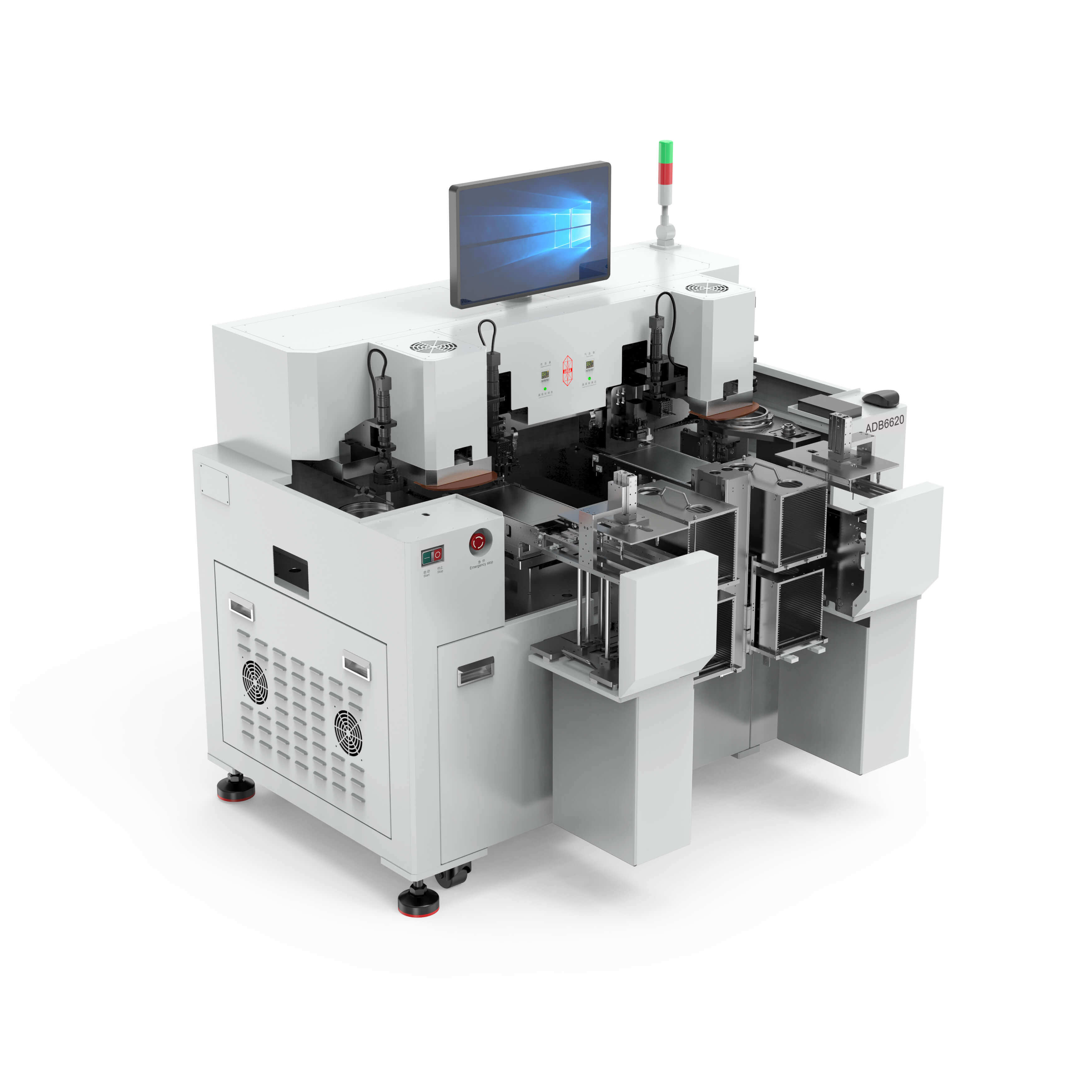
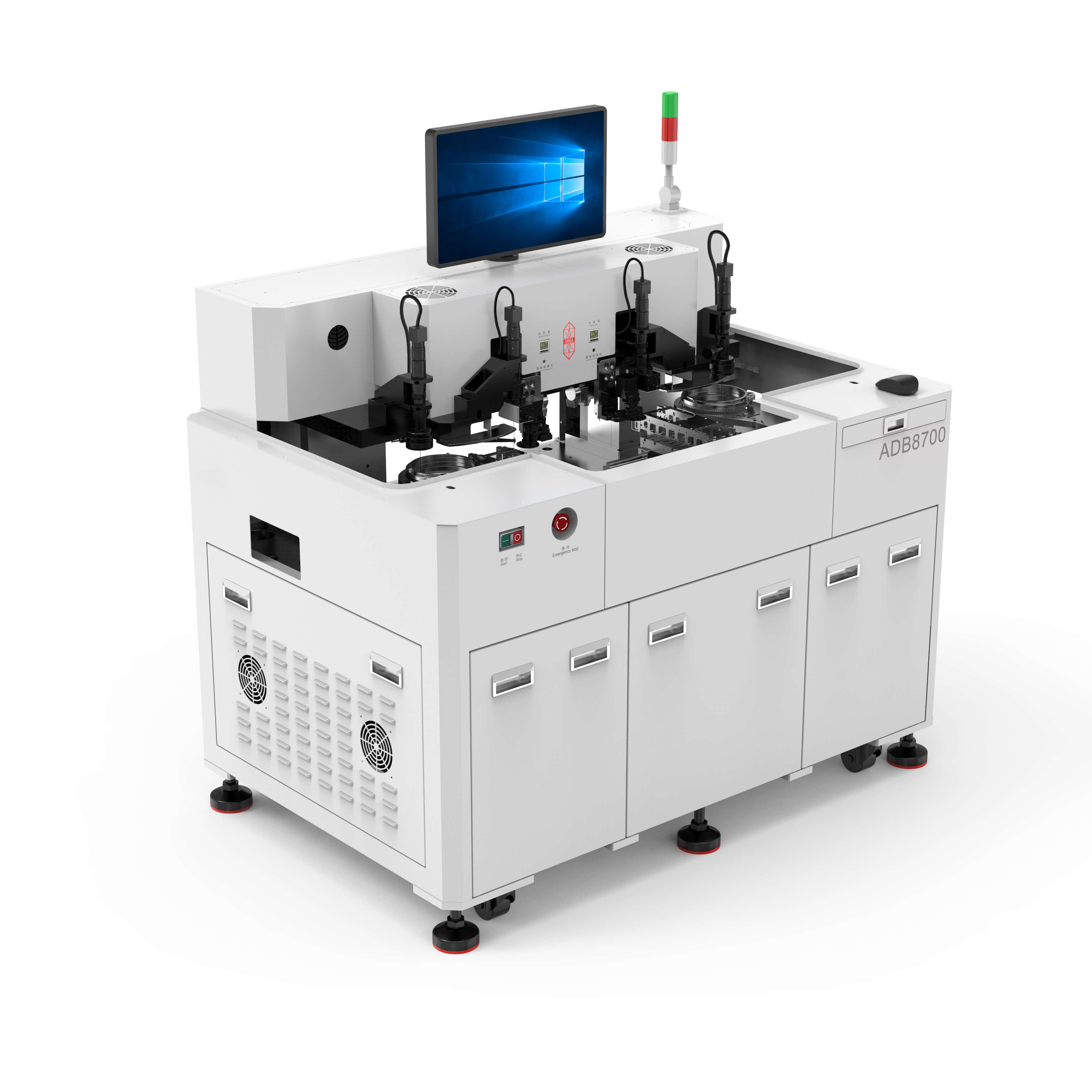
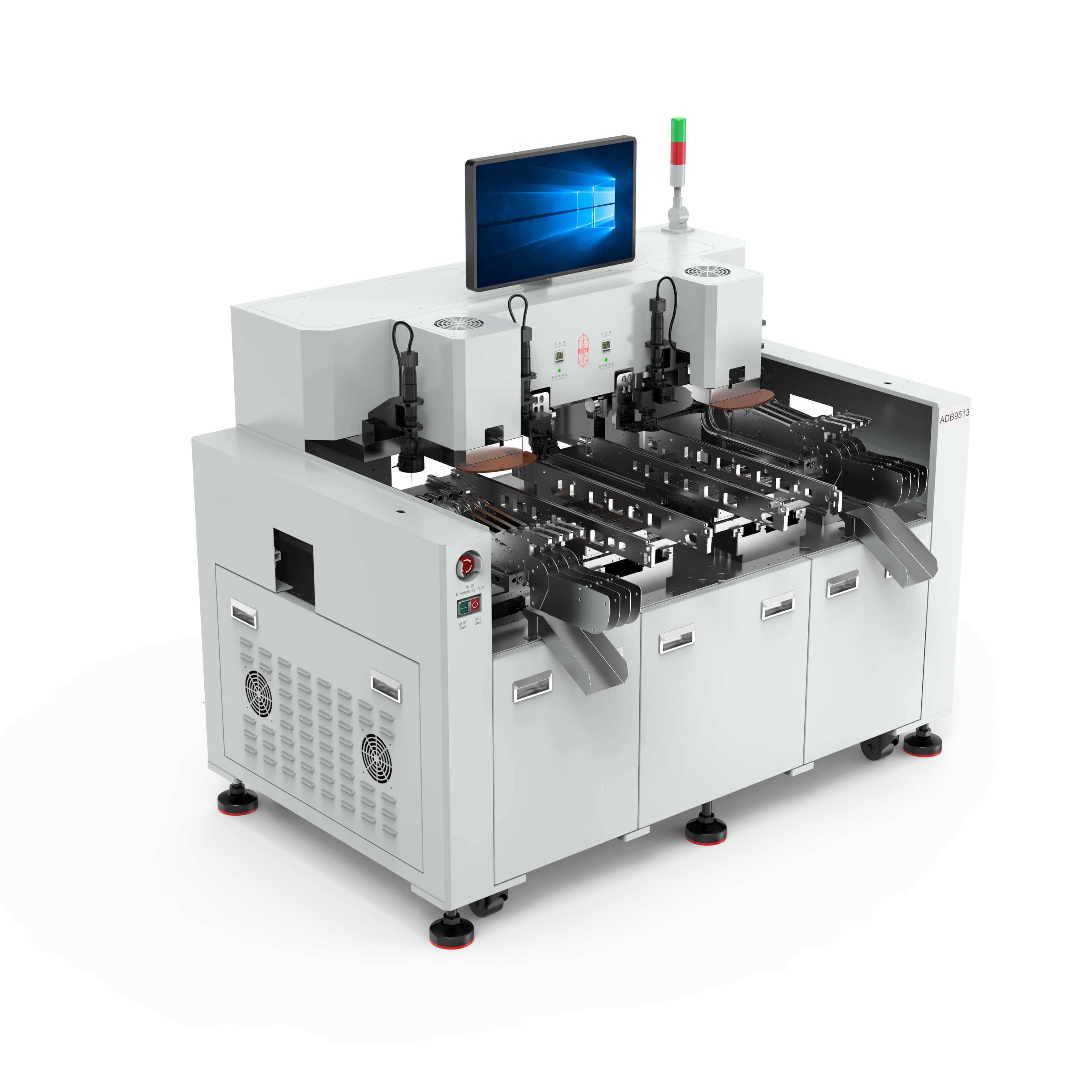
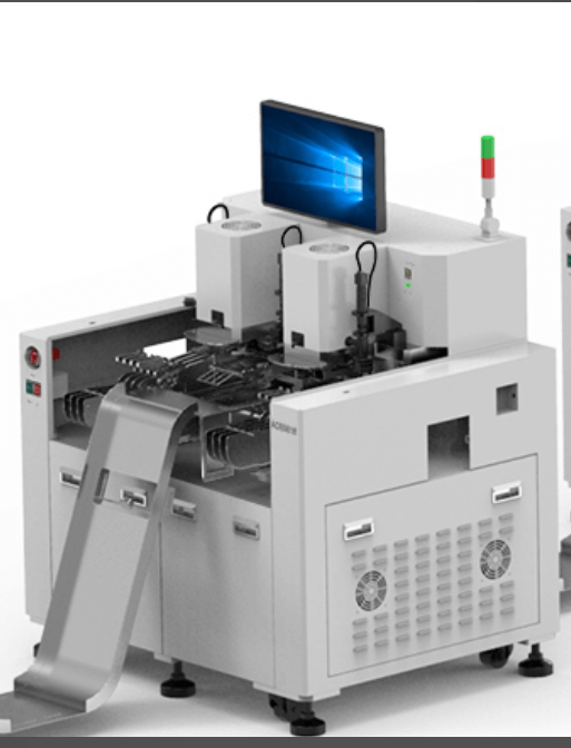
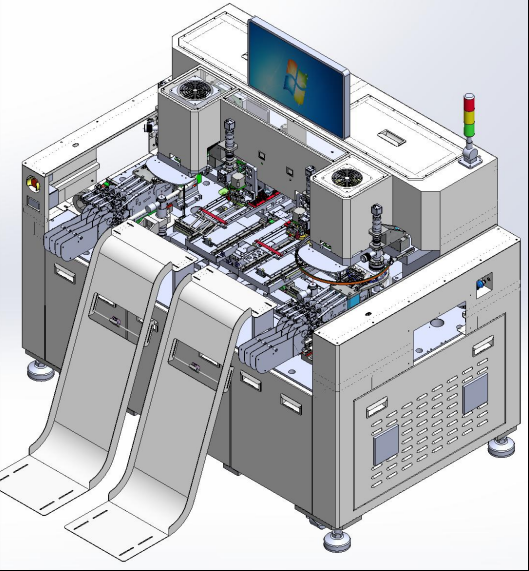
The company has a professional R&D team, overcomes many technical difficulties, and has achieved a number of self-research results. Its main product, the crystal fixing machine, integrates high accuracy, high speed and high stability, and is of high quality! It is widely used in well-known enterprises at home and abroad, and is deeply trusted and praised by customers.
According to the market and customer needs, the company integrates equipment innovation, equipment compatibility and rapid response to solve customer needs and pain points. It has obvious advantages. It gradually occupies the domestic market and is also competitive internationally, adding luster to China's high-end intelligent equipment manufacturing industry. Perfect after-sales service provides all-round support to customers, consolidating the leading position in the field.
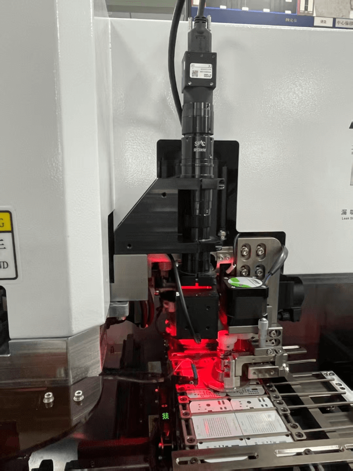

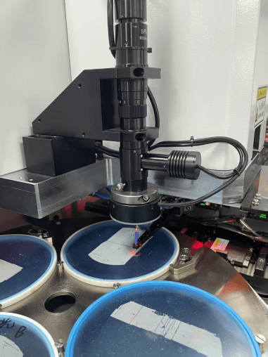
As an innovative enterprise specializing in the R&D and manufacturing of die bonders, we have become a reliable partner in certain fields, relying on solid technical accumulation and rich practical experience. All core members of the team have more than 12 years of industry experience, with professional expertise covering mechanical design, automatic control, and visual algorithm development. The team leader has deeply engaged in the R&D of die bonding equipment and accumulated mature solutions in the field of precision motion control; the technical director has over 15 years of experience in semiconductor packaging technology, leading the team to overcome the challenges of high-precision die bonding motion control algorithms, and his innovative achievements have been widely applied in the company's core products.


In recent years, with the continuous development of semiconductor technology and the increasing demand for applications, advanced packaging has become an important field to promote the upgrading of the domestic semiconductor industry. Especially with the application of innovative technologies such as 2.5D/3D packaging, Chiplet technology, and System in Package (SiP), China's advanced packaging industry is ushering in new development opportunities and gradually becoming an important part of the global semiconductor industry.
Advanced packaging refers to an innovative method that can integrate multiple chips, functions, and materials into a compact package. These include 3D stacking, System-in-Package (SiP), and Fan-Out Wafer-Level Packaging (FOWLP).
In the past month, traditional OSATs (outsourced semiconductor assembly and testing factories) such as Tongfu Microelectronics, TSMC, Amkor, ASE (Advanced Semiconductor Engineering), and Huatian Technology, as well as leading wafer fabs...